Nforce 650I Sli Bios Update
- Si tu tarjeta gráfica GeForce®/Quadro®, o tu placa base nForce® estaban integradas en un PC que has comprador.
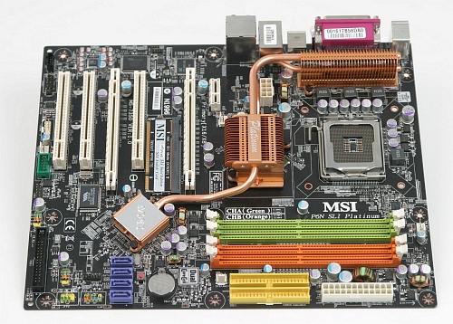
- The Intel Core microarchitecture (previously known as the Next-Generation Micro-Architecture) is a multi-core processor microarchitecture unveiled by Intel in Q1 2006.
Tested motherboards. Below you'll find a list of motherboards that have been tested with this MOD. We've also included some motherboards that should be compatible. Drivers and BIOS. Below you will find drivers for all of EVGA's current products. Simply choose from the selections below and click download for whatever version file. NForce MCPs NVIDIA nForce® media and communications processors (MCPs) are the key ingredient in the best motherboards for NVIDIA GeForce GPUs.
CPUID DEVELOPERS CORNER. The System Information Development Kit offers a set of functions that gathers in- deep information about the core components ofa PC : CPU, chipset, memory.
Intel Core (microarchitecture) - Wikipedia. This article is about the Intel microarchitecture. For Intel processors branded as Intel Core, see Intel Core.
Here are the latest articles published on Tom’s Hardware. See the latest news, reviews and roundups and access our tech archives. Free Christmas Vectors Adobe Illustrator on this page.
The Intel Core microarchitecture (previously known as the Next- Generation Micro- Architecture) is a multi- core processormicroarchitecture unveiled by Intel in Q1 2. It is based on the Yonah processor design and can be considered an iteration of the P6 microarchitecture, introduced in 1. Pentium Pro. The high power consumption and heat intensity, the resulting inability to effectively increase clock speed, and other shortcomings such as the inefficient pipeline were the primary reasons for which Intel abandoned the Net. Burst microarchitecture and switched to completely different architectural design, delivering high efficiency through a small pipeline rather than high clock speeds.
The Core microarchitecture never reached the clock speeds of the Netburst microarchitecture, even after moving to 4. Core as the basis (such as Nehalem, Sandy Bridge and more) Intel managed to surpass the clock speeds of Netburst using the Devil's Canyon (Improved version of Haswell) microarchitecture which reached a base frequency of 4 GHz and a maximum tested frequency of 4. GHz using 2. 2 nm lithography and ultimately derives from the P6 microarchitecture through the Core microarchitecture and many other succeeding improvements.
The first processors that used this architecture were code- named 'Merom', 'Conroe', and 'Woodcrest'; Merom is for mobile computing, Conroe is for desktop systems, and Woodcrest is for servers and workstations. While architecturally identical, the three processor lines differ in the socket used, bus speed, and power consumption. Mainstream Core- based processors are branded Pentium Dual- Core or Pentium and low end branded Celeron; server and workstation Core- based processors are branded Xeon, while Intel's first 6.
Core- based processors were branded Core 2. Features. Intel's CPUs have varied widely in power consumption according to clock rate, architecture, and semiconductor process, shown in the CPU power dissipation tables. Like the last Net. Burst CPUs, Core based processors feature multiple cores and hardware virtualization support (marketed as Intel VT- x), as well as Intel 6. Tomtom Us Canada Android Cracked Games.
SSSE3. However, Core- based processors do not have the Hyper- Threading Technology found in Pentium 4 processors. This is because the Core microarchitecture is a descendant of the P6 microarchitecture used by Pentium Pro, Pentium II, Pentium III, and Pentium M. The L1 cache size was enlarged in the Core microarchitecture, from 3. KB on Pentium II/III (1. KB L1 Data + 1. 6 KB L1 Instruction) to 6.
KB L1 cache/core (3. KB L1 Data + 3. 2 KB L1 Instruction) on Pentium M and Core/Core 2. It also lacks an L3 Cache found in the Gallatin core of the Pentium 4 Extreme Edition, although an L3 Cache is present in high- end versions of Core- based Xeons. Both an L3 cache and Hyper- threading were reintroduced in the Nehalem microarchitecture. Roadmap. Penryn's successor, Nehalem borrowed more heavily from the Pentium 4 and has 2.
The new architecture is a dual core design with linked L1 cache and shared L2 cache engineered for maximum performance per watt and improved scalability. One new technology included in the design is Macro- Ops Fusion, which combines two x. For example, a common code sequence like a compare followed by a conditional jump would become a single micro- op. Unfortunately, this technology does not work in 6. Other new technologies include 1 cycle throughput (2 cycles previously) of all 1. SSE instructions and a new power saving design.
All components will run at minimum speed, ramping up speed dynamically as needed (similar to AMD's Cool'n'Quiet power- saving technology, as well as Intel's own Speed. Step technology from earlier mobile processors). This allows the chip to produce less heat, and consume as little power as possible. The desktop- oriented Conroe began with models having an FSB of 8. MT/s or 1. 06. 6 MT/s with a 1. MT/s line officially launched on July 2. The power consumption of these new processors is extremely low—average use energy consumption is to be in the 1–2 watt range in ultra low voltage variants, with thermal design powers (TDPs) of 6.
Conroe and most Woodcrests, 8. GHz Woodcrest, and 4.
Woodcrest. In comparison, an AMD Opteron 8. HE processor consumes 5. Socket AM2 line fits in the 3. Merom, the mobile variant, is listed at 3. TDP for standard versions and 5 watts TDP for Ultra Low Voltage (ULV) versions.
However, at IDF in the spring of 2. Intel advertised both. Some of the promised numbers were: 2. Merom at the same power level (compared to Core Duo)4. Conroe at 4. 0% less power (compared to Pentium D)8.
Woodcrest at 3. 5% less power (compared to the original dual- core Xeon)Processor cores. For instance, code name .
Most of the mobile and desktop processors come in two variants that differ in the size of the L2 cache, but the specific amount of L2 cache in a product can also be reduced by disabling parts at production time. Wolfdale- DP and all quad- core processors except Dunnington QC are multi- chip modules combining two dies. For the 6. 5 nm processors, the same product code can be shared by processors with different dies, but the specific information about which one is used can be derived from the stepping.
Conroe/Merom (6. 5 nm). Depending on their configuration and packaging, their code names are Conroe (LGA 7. MB L2 cache), Allendale (LGA 7.
MB L2 cache), Merom (Socket M, 4 MB L2 cache) and Kentsfield (Multi- chip module, LGA 7. MB L2 cache). Merom and Allendale processors with limited features can be found in Pentium Dual Core and Celeron processors, while Conroe, Allendale and Kentsfield also are sold as Xeon processors.
Additional code names for processors based on this model are Woodcrest (LGA 7. MB L2 cache), Clovertown (MCM, LGA 7. It is used only in ultra- low voltage Core 2 Solo U2xxx and in Celeron processors and is identified as CPUID family 6 model 2. Processor. Brand name. Model (list)Cores.
L2 Cache. Socket. TDPMerom- LMobile Core 2 Solo. U2xxx. 12 Mi. BBGA4. WMerom- LCeleron M5x. Ki. BSocket MSocket P2.
WMerom- L5x. 35. 12–1. Ki. BBGA4. 79. 5. WConroe- LCeleron M4x. Ki. BLGA 7. 75. 35 WConroe- CL4x. LGA 7. 71. 65 WPenryn/Wolfdale (4. In Core 2 processors, it is used with the code names Penryn (Socket P), Wolfdale (LGA 7.
Yorkfield (MCM, LGA 7. Celeron, Pentium and Xeon processors. In the Xeon brand, the Wolfdale- DP and Harpertown code names are used for LGA 7. MCMs with two or four active Wolfdale cores. The chips come in two sizes, with 6 MB and 3 MB L2 cache. The smaller version is commonly called Penryn- 3. M and Wolfdale- 3.
M as well as Yorkfield- 6. M, respectively. The single- core version of Penryn, listed as Penryn- L here, is not a separate model like Merom- L but a version of the Penryn- 3. M model with only one active core. Dunnington. Most of these steppings are used across brands, typically by disabling some of the features and limiting clock frequencies on low- end chips. Steppings with a reduced cache size use a separate naming scheme, which means that the releases are no longer in alphabetic order. Additional steppings have been used in internal and engineering samples, but are not listed in the tables. Many of the high- end Core 2 and Xeon processors use Multi- Chip Modules of two or three chips in order to get larger cache sizes or more than two cores.
Steppings using 6. Stepping L2 and M0 are the . In mobile processors, all of which support C1 through C4 idle states, steppings E1, G0, and M0 add support for the Mobile Intel 9. Express (Santa Rosa) platform with Socket P, while the earlier B2 and L2 steppings only appear for the Socket M based Mobile Intel 9. Express (Napa refresh) platform. The model 2. 2 stepping A1 (cpuid 1. Mi. B L2 cache further reducing the power consumption and manufacturing cost for the low- end.
Like the earlier steppings, A1 is not used with the Mobile Intel 9. Express platform.